
Contact
Write to Us And We Would Be Happy to Advise You.
Do you have any questions, or would you like to speak directly with a representative?
By hqt
Raw materials used in the fabrication process include High strength low Alloy Steel (HASL) and gold sunk plates, which are all popular raw materials in today's PCB industry. HASL prevents the oxidation on the surface of copper maintaining its properties for processability. Gold plating gives stability and colour and also creates a flattened coated surface that produces a good effect on the printed circuit.
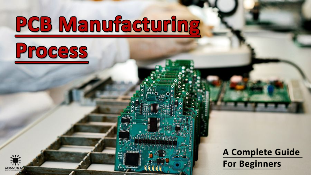
PCB manufacturing is a very important process because it has a great impact on the accuracy of raw material manufacturing.
Let’s discuss PCB manufacturing processes in detail.
The main step for the production is to make its PCB design. Some software has developed new features, and we just need a few clicks to complete the design. In this way, it is easy to draw designs without the help of paper and pen. Most widely used designing software includes Auto CAD, MAT lab, Eagle, etc.
We can design the choices we need through this software. The software automatically checks to reduce the chance of errors. It also checks for the symbols that are generated during the process.
The manufacturer receives the finished designs and approves them for production.
After the examination of the design, the manufacturer converts the design into film with the help of printers. And the printers are used in the production of photo films. These films print PCB circuit boards and they will use these films for imaging PCB. They would then acquire a highly detailed, precise PCB design membrane.
The required product is in the form of plastic sheet electrons on its surface and this appears in form of black ink. This black ink shows conductive parts while another clear portion indicates the non-conductive part of PCB.
The black portion is the one that will be etched further while the outer layers are clear in the case of copper. Moreover, the printer also develops a coating that serves as protecting a thin layer concerning the surrounding. Hence, the film can be stored easily.
To remove the unwanted copper, we prepared an alkaline solution. As the hard resistance layer that we need to cover copper is removed, the bare plate enters the next stage. This alkaline solution is very powerful and hence removes all the unwanted copper while the desired Cu remains protected under the photo-resistant film.
The inner and outer layers require alignments so that processing can become easy. At this time we need an optical punch to do the job. Once layers are aligned with one another it is difficult to separate them. Original design in form of a file received by a printed circuit board manufacturer serves as an example.
If it shows an inconsistency, it appears on the screen. Then we can correct it very easily.
After the alignment, bonding and layering of outer layers with the substrate molecules occurs. This outer layer consists of a thin fiber sheet aligned with epoxy resin. Thin Cu foil protects and covers both sides of substrate molecule that contain elements of Cu for etching.
Then they are fused and result in bonding. The substrate molecule attaches to the film before the placement of Cu. Now an Al foil and copper foil form a complete fused surface ready to be pressed.
This stack is heated by applying pressure and then allowed to cool under required conditions. This will cause little unpacking and hence we get the required multi-layer product.
PCB circuit board manufacturer drills holes on the circuit board. These holes have very small widths and diameters. All components that are to be connected with it, are linked through these holes.
An X-ray detector or some optical inspection methods are used to find the exact drilling spot. Every small movement of the drill is controlled with the help of computers. Such machines use original file designs to identify particular drill spots.
When the drilling is complete, they use analytical tools to remove the extra copper.
In this process, the manufacturer will be plating the film. Chemical deposition occurs resulting in the fusion of outer and inner layers. After a series of treatments, its surface creates a thin layer of copper deposits. So copper can be drilled into the hole.
After this, the manufacturer images the outer layer. They applied the light-resistant film to the film and then transported it to the yellow chamber. Because if the yellow light does not have enough wavelength, it can affect the film.
Moreover, the copper is redeposited on the surface of the film, and the outer layer receives this coating, allowing the remaining copper to be removed. It serves as protecting layer for the film to remain covered during further processing.
During the final etching process, the high-quality tin protects the copper required during the process. During this removal process, the unexposed and unwanted copper also disappeared. Then, for the surface finish, they use a chemical solution to remove the excess copper. Similarly, the material tin protects the copper and keeps it in good shape.
In this process of PCB manufacturing, the next step that comes is the procedure of solder masks. First, clean the panel, and then cover both sides of the plate using an epoxy solder mask ink.
The injected ultraviolet light is then emitted onto it, and the process is through the solder mask photo film. Also, sometimes those parts that are covered in the outer layer will remain unchanged, i. e., unhardened. And they will end up in the process of removal.
To make it a high-quality, more durable product, manufacturers need to perform chemical plating. The material required for the chemical plating process is either gold or silver. Some printed circuit board receives the hot air-level pads in this stage which leads to uniform pads. All of this leads to the procedure of surface finish.
At this point, the board receiving inkjet process is almost complete and is about to convert. The PCB design finally then passes to the last stage which is the stage of coating and curing.
Because the last part is undergoing electrical testing on the PCB, make sure that there is no error in the previous process. In this process, the manufacturer needs to confirm the functionality of the PCB to ensure that it fits the original PCB prototype.
The question that arises is whether the fabrication process is necessary to understand or not. Because this process is part of the PCB layout or design process, some specification issues are important. Manufacturers need to be aware of these issues before making specific designs. Then the factory can carry out the specific design.
Customers do not understand the high-quality source of these products until they fully understand the entire manufacturing process. Once you fully understand the process, you can decide accordingly on the outer layer, materials, PCB layout, optical inspection, etc. As it can impact the overall performance of PCB assemble and its manufacturability.
A good service provider is necessary if you are looking for a high-quality product. The layout of the PCB and even the whole manufacturing process is very complex. So we need more professional factory equipment to run the PCB manufacturing process.
Europe PCB, known as one of the great service providers of PCB assembly manufacturers all around Europe, provides the best services. They can provide their services in SMT & DIP and much more.
Do you have any questions, or would you like to speak directly with a representative?