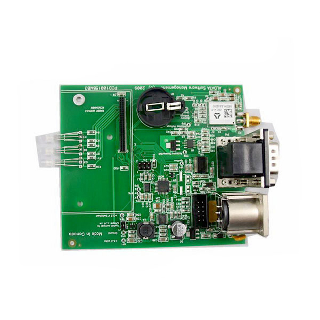
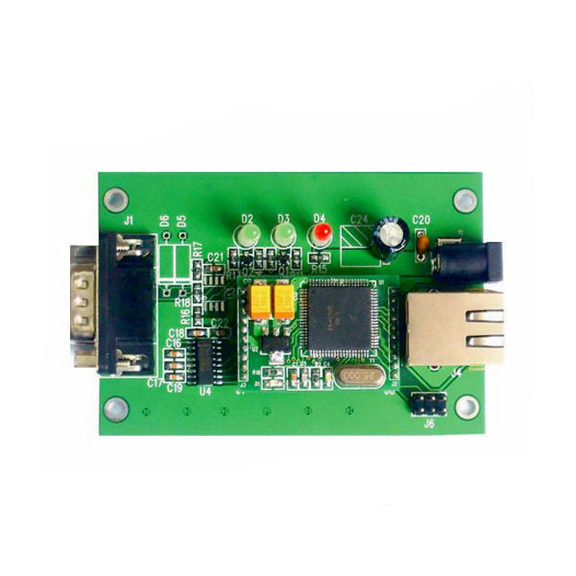
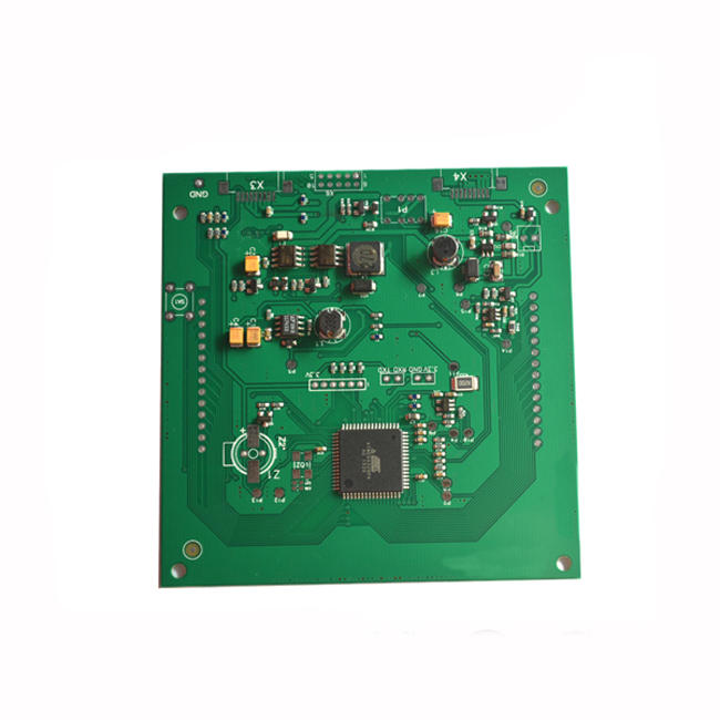
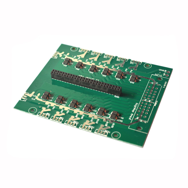
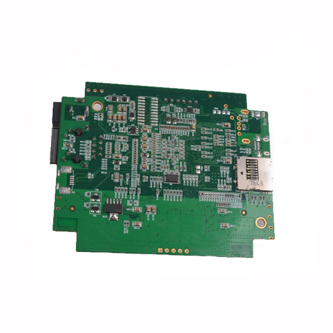
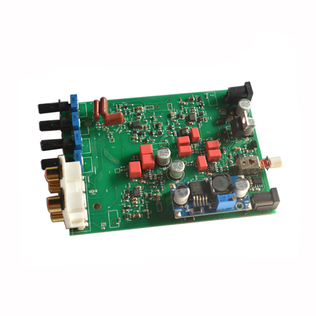
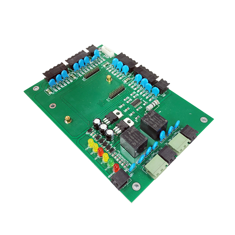
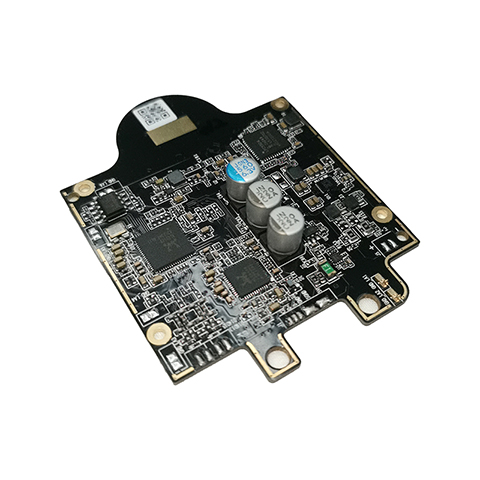
Electronics are an integral part of our daily lives. Everything from smartphones to cars contains electronic components. At the heart of these electronics is the printed circuit board, also known as the PCB. Most people recognize it when they look at the circuit board. These are the small green chips covered with wires and copper pieces at the heart of human-eating electronics.
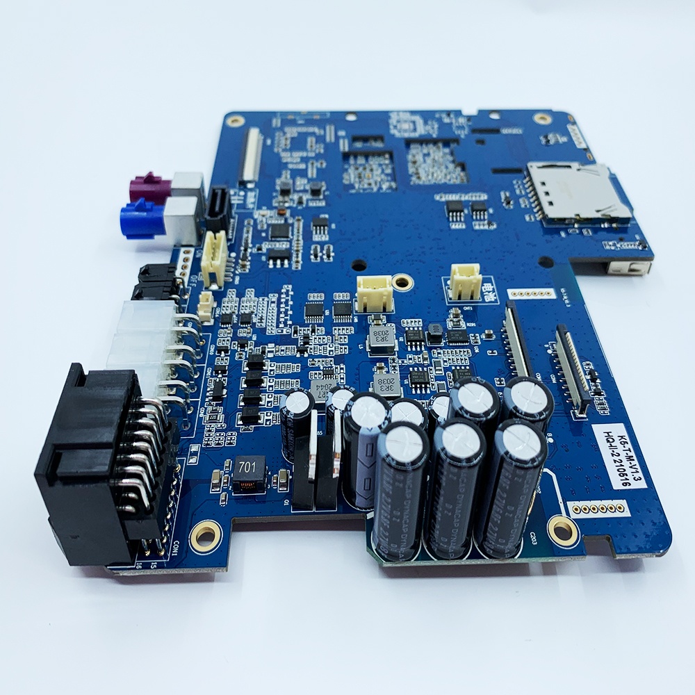
These boards are made of fiberglass, copper wire, and other metal parts, fixed with epoxy resin and insulated with a solder mask. But have you ever seen these boards with the components firmly glued together? Don't think of them the same as the decoration of printed circuit boards. Advanced printed circuit boards will not function properly until the components are installed. The circuit board with the components attached is called the assembled circuit board, and the manufacturing process is called the PCB assembly or PCBA for short.
PCB Assembly Overview:
Did you know that almost every gadget or electronic device we use in our daily life has a common basic building block? Almost all electronic devices, including computers, laptops, smartphones, game consoles, microwaves, TVs, dishwashers, and more, will not work without assembling a circuit board.
So, what is PCB assembly?
PCB Assembly is an abbreviation for several assembly processes for components on a PCB board, and PCB is a printed circuit board. SMT is a surface mount technology (surface mount technology) that is the most popular technology and process in the electronics assembly industry. The technology of assembling printed circuit boards is called surface mount technology. It is a type of PCB assembly technology in which loose or short lead assembly components are mounted to the surface of a PCB or other board and assembled by reflow soldering or immersion welding.
Current PCB assembly status:
European and American customers find PCB assembly difficult.
First, high cost and long delivery times are always an issue when prototyping PCBs for European and American customers. This is because a limited number of local PCB manufacturers are struggling to keep up with market demand, and few manufacturers can provide comprehensive PCB assembly services. If the customer assembles the PCB in their own country, it can cost much more and take more time. Also, it is difficult to assemble a PCB abroad due to language and cultural differences.
For example, many foreign trading companies can provide PCB assembly services. However, there are not many people who can speak a foreign language and PCB manufacturing technology at the same time. So, finding the right PCB manufacturer is not an easy task.
Turnkey PCB assembly services have become a major trend in China. To meet increasing demand and improve market competition, many PCB assembly manufacturers provide turnkey services to domestic and international customers.
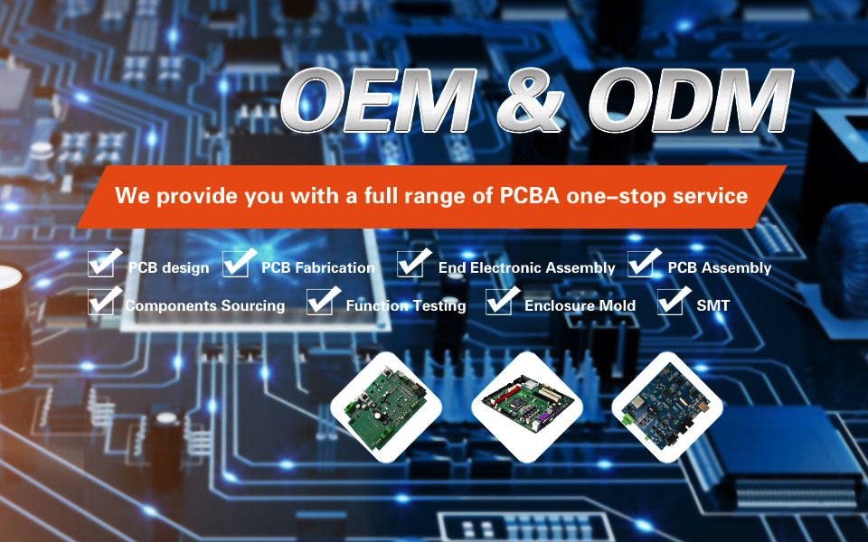
For example, PCBGOGO is a professional PCB manufacturer that can provide full services of PCB manufacturing, component sourcing, PCB assembly, and PCB testing for European and American customers. Turnkey Services reduces the time customers spend contacting multiple suppliers for specific steps in PCB assembly.
And our scientific ordering system allows our customers to get higher quality and lower cost PCB assembly products in less time than traditional PCB assembly. Our turnkey service allows you to create a PCB prototype in 12 hours and assemble a PCB prototype in 24-7 hours even with minimum quantity requirements. Of course, PCB fabrication, component sourcing, and PCB assembly services can be selected separately or in combination with each other.
Before the PCB Assembly Process:
Several preparatory steps need to be taken before the actual PCBA process begins. This helps PCB manufacturers to evaluate the functionality of their PCB designs and mainly includes DFM verification.
Most PCB assembly companies need other design notes and special requirements along with the PCB design file to get started. This is to allow PCB assembly companies to check their PCB files for issues that may affect the functionality or manufacturability of the PCB. This is a design to test manufacturability. In short, it is the DFM test.
DFM inspection verifies all design characteristics of the PCB. Specifically, this check looks for missing, duplicate, or potentially problematic features. These issues can seriously and negatively affect the functionality of the final design. For example, one of the common design flaws in printed circuit boards is that the spacing between components is too small. Short circuits and other malfunctions may occur.
By identifying potential problems before manufacturing begins, DFM checks can cut manufacturing costs and eliminate unforeseen expenses. This is because these checks cut down on the number of scrapped boards. As part of our commitment to quality at a low cost, DFM checks come standard with every PCBCart project order. PCBCart provides FREE DFM and DFA check with, however, priceless values because Valor DFM/DFA check Europe PCB depends on is an automatic system contributing to high speed and accuracies.
Manufacturing Process of PCB Overview:
1. Solder Paste Application In automatic assembly, the solder stencil is held in place on the board and the applicator applies the correct amount of solder paste where needed. Since the stencil is a thin sheet of metal with holes, the solder paste should only be applied to the part of the PCB where the components will be placed. Solder paste is a mixture of solder (small balls of metal) and flux (a chemical that helps the metal melt and adhere better to a surface).
2. Pick and Place (SMT) Once the solder is applied, the board moves to the pick and place (PNP) machine. This machine automatically orients the board and places components onto the solder paste using preprogrammed locations. With surface mount technology (SMT), components are soldered only to the surface of the board. Today, the majority of non-connector components are mounted with SMT because PNP machines are extremely fast and accurate.
3. Reflow soldering After the components are placed, the board is moved to the reflow oven. The oven gradually heats the board to melt the solder paste to create a permanent connection between components and boards, then cools the board in an equally controlled manner to prevent damage from shock.
4. Inspection and Quality Assurance Errors in the previous process can result in components that are not connected, shorts in the board, or misaligned components. Inspections ensure errors and found and corrected as quickly as possible, preventing costly delays. There are various inspection methods, such as manual inspection by humans, automatic optical inspection by image recognition, and X-ray inspection to see parts that may block the inspector's field of vision.
5. Through-hole technology (THT) parts may be required in addition to SMT parts depending on the insert board. Some elements, such as headers and larger components, are only available in THT. Since the pins of these components pass through the holes in the board, they cannot be used as long as the solder paste passes through the holes without sticking. Instead, THT uses wave soldering. Here, the machine creates a wave of solder on the tray that washes the bottom of the board and solders all the pins on the bottom of the board at the same time.
6. Final inspection and functional testing. After soldering is complete, the PCB is tested under normal operating conditions. This is the most important step in the PCB assembly process to ensure that only high-quality PCBs are delivered to the customer.
After PCB assembly:
It is enough that the PCB assembly process can be messy. The solder paste leaves a little flux, and if a person is exposed, grease and dirt can flow from fingers and clothing onto the PCB surface. When everything is done, the result can look a bit messy. This is an aesthetic and practical matter. After a few months on the PCB, the remaining flux will start to swell and become sticky. It also becomes somewhat acidic which can damage solder joints over time. Additionally, customer satisfaction tends to suffer when new PCB shipments are covered in debris and fingerprints. For this reason, it is important to clean the product after completing all soldering steps.
A stainless steel high-pressure washer with deionized water is the best tool for removing residues from PCBs. Cleaning the printed circuit board with deionized water is not hazardous to the device. The reason is that the damage in the circuit is not caused by the water itself, but by the ions in the ordinary water. Therefore, deionized water is harmless to PCBs undergoing cleaning cycles. After cleaning with a fast compressed air drying process, the finished PCB remains ready for packaging and shipping.
Why choose Europe PCB for PCB assembly overview?
To optimize customer expectations for both product performance and return on investment, the Europe PCB began offering PCB manufacturing and assembly services under one roof a few years ago. Combined with ISO9001, TS16949, UL, and RoHS certifications and years of experience in this industry, and over 99% customer satisfaction, we have a high enough PCB assembly capability to provide high-quality assembly services following very stringent quality standards and regulations.


